Featured Post Today
print this page
Latest Post

Pulse Rate Monitor Circuit Diagram

Description
This simple circuit enables you to listen to your heartbeat, for instance, while you are exercising. The transducer used for detecting the pulse is an electret microphone, X1 in the diagram. The model used has two (polarized) terminals. As usual with this type of microphone, it functions via a series resistor, R1. The potential drop across this resistor is applied to op amp IC1a via C1. The amplification of the op amp is set to between ´40 and ´1000 with preset P1. Network R4-C3 in the feedback loop of IC1a is a low-pass filter with a cut-off frequency of 34 Hz. Higher frequencies are not needed for the present application. A pulse rate of 180* is equivalent to a frequency of 3 Hz.

So as to cater for a wide range of pulse rates, the cut-off frequency is made just over 11 times as high as that representing the highest pulse rate. Operational amplifier IC1c, in conjunction with push-pull am-plifier T1-T2, creates a headphone amplifier, whose output resistance is equivalent to the value of R9, that is, 47 Ω. This makes the circuit usable for virtually any kind of headset. The output is short-circuit-proof. In case of certain headphones, such as that used with Sony Walkman™ sets, it is best to connect the two earphones in series. Operational amplifier IC1b is used as an active potential divider. The voltage across the actual divider, R5-R6, is half the supply voltage.
Circuit Diagram
This voltage is buffered by IC1b, taken from the low-resistance output, pin 7, of this op amp and used as reference for IC1a, and as operating voltage for the electret microphone. The voltage is decoupled by C4 to remove any interference signals from it. The supply voltage for the pulse rate monitor is decoupled by capacitor C7, immediately after polarity protection diode D1. Owing to the use of CMOS op amps, the current drain does not exceed 10 mA, so that operation from a 9 V battery is perfectly feasible. A dry alkaline manganese battery will have a life of about 50 hours.

Unless you are a young superfit top-class athlete, you should see your GP immediately when you find you have a pulse rate of 180. As a general guide, the absolute maximum pulse rate for a young, very fit person is 180, for a middle-aged person, 160, and for an elderly person, 140. When exercising, the pulse rate of a not very fit person should not exceed 60% of these maxima.
0 comments

Single Zone Alarm Circuit Diagram

Description:
 A single zone alarm circuit with entry and exit delay and other facilities.
Circuit Diagram
Notes:
The circuit features automatic exit and entry delays, timed bell cut-off and system reset. It has provision for normally open and normally closed switches and will suit the usual input devices (Pressure Mats, Magnetic Reed contacts, Foil Tape, PIRs and Inertia Sensors). When the power is applied, if there's a fault the buzzer will sound and you should switch off again and check for open doors, windows, etc. If everything is in order the buzzer will NOT sound and the exit delay will begin. You have about 30 seconds to leave the building. When you return the buzzer will sound. You then have about 30 seconds to switch off; otherwise the siren will sound. It will go on sounding indefinitely. However, if the building is re-secured the siren will switch off after about 10 minutes and the alarm will reset.
The Exit delay, Entry delay and Bell Cut-off times can be changed by altering the values of R4, R12 & R13 respectively. Q5 and Q6 ensure that the Entry delay and Bell cut-off timers always start with C7 either fully charged or fully discharged as required. If you can live with slightly less precise time intervals then leave out Q5, Q6, R14, R15, R16, R17, C8 & C9. If you don't want a Bell Cut-off at all then leave out D3 as well.
The sensitivity of the Inertia Sensors is adjusted by R8. Set to minimum value, a light tap will activate the alarm. Set to maximum value, a heavy blow is required. If you are not using Inertia Sensors then replace R8 with a 27k fixed resistor. If you are not using normally open switches then leave out R1, C1 & Q1 and fit a link between R2 and C2.
Board Layout:
 Source - http://www.zen22142.zen.co.uk/Circuits/Alarm/sza.htm
0 comments

IC Controlled Emergency Light With Charger Circuit Diagram

Circuit Diagram: 
Description
Here is the circuit diagram of IC Controlled Emergancy Light With Charger or simply 12V to 220V AC inverter circuit. The circuit shown here is that of the IC controlled emergency light. Its main features are: automatic switching-on of the light on mains failure and battery charger with over-charge protection. When mains is absent, relay RL2 is in de-energized state, feeding battery supply to inverter section via its N/C contacts and switch S1.
The inverter section comprises IC2 (NE555) which is used in stable mode to produce sharp pulses at the rate of 50 Hz for driving the MOSFETs. The output of IC2 is fed to gate of MOSFET (Q4) directly while it is applied to MOSFET (Q3) gate after inversion by transistor Q2. Thus the power amplifier built around MOSFETs Q3 and Q4 functions in push-pull mode. The output across secondary of transformer T2 can easily drive a 230-volt, 20-watt fluorescent tube. In case light is not required to be on during mains failure, simply flip switch S1 to off position. Battery overcharge preventer circuit is built around IC1 (LM308).
Its non-inverting pin is held at a reference voltage of approximately 6.9 volts which is obtained using diode D5 (1N4148) and 6.2-volt zener D6. The inverting pin of IC1 is connected to the positive terminal of battery. Thus when mains supply is present, IC1 comparator output is high, unless battery voltage exceeds 6.9 volts. So transistor Q1 is normally forward biased, which energises relay RL1. In this state the battery remains on charge via N/O contacts of relay RL1 and current limiting resistor R2. When battery voltage exceeds 6.9 volts (overcharged condition), IC1 output goes low and relay RL1 gets de-energised, and thus stops further charging of battery. MOSFETs Q and Q4 may be mounted on suitable heat sinks. 
Parts:

  • R1 = 1K
  • R2 = 10R-1W
  • R3 = 820R
  • R4 = 1K
  • R5 = 10K
  • R6 = 1K
  • R7 = 100R
  • R8 = 1K
  • C1 = 1000uF-25V
  • C2 = 10uF-16V
  • C3 = 0.01uF
  • D1 = 1N4007
  • D2 = 1N4007
  • D3 = 1N4007
  • D4 = 1N4007
  • D5 = 1N4148
  • D6 = 6.2V Zener
  • D7 = 1N4007
  • D8 = 1N4148
  • Q1 = SL100
  • Q2 = 2N2222
  • Q3 = IRF840
  • Q4 = IRF840
  • IC1 = LM308
  • IC2 = NE555
  • S1 = SPST Switch
  • B1 = 6V-4A Battery
  • B2 = 6V-4A Battery
  • TI = 220V AC Primary to 0V-6V 250mA Secondary Transformer
  • T2 = 4.5V-0V-4.5V 5A Primary To 230V AC Secondary Transformer 
Source - http://www.extremecircuits.net/2010/01/ic-controlled-emergency-light-with.html
0 comments

Digital AC/DC Voltage Tester Circuit Diagram

Description
It is always necessary for engineers and technicians to test AC/DC mains voltages and continuity for any given circuit during breakdowns, the above mentioned circuit can be used as and sought of tester and can also check the continuity for you. all one has to do is that to touch the two probes at the required terminal of either live or an dead circuit
The unique design of the tester allows the circuit to work in both AC and DC without any mode selector switch.
When the probes A and B are short circuited voltage pin 1 goes a little below the threshold of the Schmitt trigger due to the voltage divider action of the resistor R1, R2 and VR1 This disables the gate of pin1 and due to this the transistor T2 goes into saturation while the transistor T1 is cut off therefore the green LED glows while the red segment goes off and the display will now glow as “C” 
 Circuit Diagram

VR1 is a miniature preset which is to be calibrated before use its calibrations are fairy simple, keep both the probes A and B short circuited and the preset VR1 at its minimum value and slowly increase the resistance value of the VR1 till the red LED glows OFF and only green LED glows

Source http://www.electronguide.com/circuits_pages/Digital_AC-DC_Voltage.html
0 comments

300W Subwoofer Power Amplifier Wiring Circuit Diagram


Circuit Diagram

Description
Please agenda that the blueprint for this amp has been upgraded, and it is now recommended for connected aerial ability into 4 Ohms, but You will charge to go to extremes with the heatsink (fan cooling is awful recommended). It was originally advised for “light” alternate duty, acceptable for an equalised subwoofer arrangement (for archetype application the ELF assumption – see the Project Page for the advice on this circuit). Where connected aerial ability is required, addition 4 achievement transistors are recommended, active in the aforementioned way as Q9, Q10, Q11 and Q12, and application 0.33 ohm emitter resistors.
Continuous ability into 8 ohms is about over 150W (250W for ±70V supplies), and it can be acclimated after added transistors at abounding ability into an 8 ohm amount all day, every day. The added transistors are alone bare if you appetite to do the aforementioned affair into 4 ohms at best accumulation voltage! Do not alike anticipate about application food over ±70V, and don’t bother allurement me if it is ok – it isn’t!
The ambit is credible in Figure 1, and it is a analytic accepted design. Connections are provided for the Internal SIM (published abroad on the Project Pages), and clarification is provided for RF aegis (R1, C2). The ascribe is via a 4.7uF bipolar cap, as this provides lots of capacitance in a baby size. Because of the impedance, little or no abasement of complete will be apparent. A polyester cap may be acclimated if you adopt – 1uF with the nominal 22k ascribe impedance will accord a -3dB abundance of 7.2Hz, which is absolutely low abundant for any sub.

Source For Updating -http://sound.westhost.com/project68.htm
0 comments

Bells Ring Generator Circuit Schematic Diagram

Description
This circuit generates a dual-tone bells ringing similar to most door-bell units. It can be used in many applications other than door-bell. In the Notes below several options will be given in order to suit different needs. The circuit as shown in the diagram generates a "Ding-tone" when P1 is pressed and a "Dong-tone" when P1 is released. IC1D is the first-tone frequency generator and IC1F generates the second-tone. Q2, Q5 and related components act as shape and decay controls of the two tones, trying to imitate as close as possible the bells sound. Their outputs are mixed (R7 & R13), filtered (C5) and boosted by a simple class-A audio amplifier (Q3 & Q4) in order to drive the loudspeaker. The amplifier is switched-on by Q1 when P1 is pressed, then is switched-off some seconds after P1 is released: this time-delay is fixed by C1 & R2. In this way the circuit will draw a negligible current when in stand-by mode. 
 Circuit Schematic Diagram
 Part
  • R1,R3,R7,R9,R13_10K 1/4W Resistors
  • R2_______________1M5 1/4W Resistor
  • R4______________27K 1/4W Resistor
  • R5,R11__________47K 1/4W Resistors
  • R6,R12_________220K 1/4W Resistors
  • R8_______________2M2 1/4W Resistor
  • R10_____________33K 1/4W Resistor
  • C1_______________2µ2 25V Electrolytic Capacitor
  • C2______________47µF 25V Electrolytic Capacitor
  • C3,C8___________10µF 25V Electrolytic Capacitors
  • C4,C7___________10nF 63V Polyester Capacitors
  • C5,C6__________100nF 63V Polyester Capacitors
  • C9_______________4µ7 25V Electrolytic Capacitor
  • C10______________1µF 25V Electrolytic Capacitor
  • D1-D5_________1N4148 75V 150mA Diodes
  • IC1__________MC14106 or 40106 Hex Schmitt Inverter IC
  • Q1_____________BC337 45V 800mA NPN Transistor
  • Q2,Q3,Q5_______BC238 25V 100mA NPN Transistors
  • Q4 ____________BC327 45V 800mA PNP Transistor
  • PH______________Photo resistor (any type) (see Notes)
  • P1______________SPST Pushbutton (see Notes)
  • SW1_____________SPST Switch
  • SPKR____________8 Ohm Loudspeaker
  • B1______________3V Battery (two 1.5V AA or AAA cells in series etc.)
  • Parts added to optional modification:
  • R14____________220K 1/4W Resistor
  • R15______________1M 1/4W Resistor 
 Notes:

  • To obtain a "Ding-Dong" operation when pushing on P1, no matter when it is released, you must modify the circuit as shown in the frame placed at the low-right corner of the circuit diagram. D4 must be removed. C10 & R15 set the time-delay separating first and second tone.
  • To obtain a one-tone-only generator, wire the circuit as in the optional modification, making the following changes:
  • C9 = 100nF 63V Polyester Capacitor.
  • Omit R9 to R13 & R15; C7, C8 & C10; D2, D4, D5 & Q5.
  • Connect to negative supply pins 11 & 13 of IC1 and left open pins 10 & 12.
  • An amusing application of this circuit wired as in the original schematic, is to use a photo-resistor in place of P1, then placing the unit near the flashing lamps of your Christmas tree. A soft bell sound may be heard at switch-on and switch-off of the lamp chosen.
  • To obtain higher output power you may substitute R8, Q3 & Q4 with an audio amplifier IC like the LM386 or LM380. In this case power supply must be raised to 6 - 12V but at the same time R4 & R10 should be changed to adjust bell-tone frequencies.
  • Good tone frequencies are roughly 2000 and 1650Hz respectively.
  • When in stand-by mode, current drawing of the circuit is 200µA @ 3V supply: therefore SW1 can be omitted.
0 comments

Basic Low Power AM Transmitter Circuit Schematic Diagram

Description
This transmitter is basic but allows transmission of audio to an AM radio. It consists of an RF oscillator operating in the AM broadcast band, together with a modulator stage, which mixes the incoming audio and the RF. A signal appears on the output, which has an AM component that can be picked up on a nearby AM radio receiver.
Circuit Schematic Diagram

The transmitter consists of oscillator stage Q1 and modulator/buffer stage Q2. Q1 is biased via R1, R2, and R3. L1, C3, and C4 form the tank circuit with feedback network C3-C4 providing feedback to the emitter of Q1. RF voltage at the junction of C3 and L1 drives buffer/modulator stage Q2. Q2 is biased by base current produced by RF rectification in the base emitter junction of Q2. C6 is an RF and AF bypass capacitor. C9, C10, and L2 form the tank circuit for the collector of Q2. RF is taken from the junction of C9 and C10 and fed to a short-wire antenna. Audio is fed to modulator Q2 via C8 and isolation resistor R5 and mixes with the RF signal in the collector circuit of Q2, producing a signal that has sum and difference frequencies if the RF carrier and AF input  along with the carrier signal.
An AM signal appears at the collector of Q2. Audio with an RMS voltage equal to about 0.7 times the collector voltage of Q2 is needed for full modulation of the output. Because of the high level of audio needed, the modulation obtained from this circuit is somewhat limited with conventional audio sources because several volts of audio into a few hundred ohms is needed. The circuit demonstrates the principle of an AM transmitter, however, and with a suitable audio drive level, produces a well modulated AM signal.

0 comments

Door Phone Circuit Schematic Diagram

Circuit Schematic Diagram
Description
This circuit can be used in front doors for visitors to communicate or it can be wired up in the front gate for conversation, this circuit is fairly simple but its worth, it dose not use any sought of condenser mic for voice transmission if uses the speaker for both the transmission purpose and for the reception purpose, the heart of the circuit is the operational amplifier LM386 which is used to amplify the voice signal gain adjust is provided by the 5k preset and the pot resistor 10k is used as the volume control.

Source - http://www.electronguide.com/circuits_pages/Doorphonecircuit.html
0 comments

AC Line Current Detector Circuit Schematic Diagram

Description
This circuit will detect AC line currents of about 250 mA or more without making any electrical connections to the line. Current is detected by passing one of the AC lines through an inductive pickup (L1) made with a 1 inch diameter U-bolt wound with 800 turns of #30 - #35 magnet wire. The pickup could be made from other iron type rings or transformer cores that allows enough space to pass one of the AC lines through the center. Only one of the current carrying lines, either the line or the neutral should be put through the center of the pickup to avoid the fields cancelling. I tested the circuit using a 2 wire extension cord which I had separated the twin wires a small distance with an exacto knife to allow the U-bolt to encircle only one wire.
The magnetic pickup (U-bolt) produces about 4 millivolts peak for a AC line current of 250 mA, or AC load of around 30 watts. The signal from the pickup is raised about 200 times at the output of the op-amp pin 7 which is then peak detected by the capacitor and diode connected to pin 7. The second op-amp is used as a comparator which detects a voltage rise greater than the diode drop. The minimum signal needed to cause the comparator stage output to switch positive is around 800 mV peak which corresponds to about a 30 watt load on the AC line. The output 1458 op-amp will only swing within a couple volts of ground so a voltage divider (1K/470) is used to reduce the no-signal voltage to about 0.7 volts. An additional diode is added in series with the transistor base to ensure it turns off when the op-amp voltage is 2 volts. You may get a little bit of relay chatter if the AC load is close to the switching point so a larger load of 50 watts or more is recommended. The sensitivity could be increased by adding more turns to the pickup. 
Circuit Schematic Diagram


0 comments

Amplifier Timer Circuit Schematic Diagram

Description 
This circuit turns-off an amplifier or any other device when a low level audio signal fed to its input is absent for 15 minutes at least. Pushing P1 the device is switched-on feeding any appliance connected to SK1. Input audio signal is boosted and squared by IC2A & IC2B and monitored by LED D4. When D4 illuminates, albeit for a very short peak, IC3 is reset and restarts its counting.
Pin 2 of IC3 remains in the low state, the two transistors are on and the relay operates. When, after a 15 minutes delay, no signal appeared at the input, IC3 ends its counting and pin 2 goes high. Q1 & Q2 stop conducting and the relay switches-off. The device is thus completely off as also are the appliances connected to SK1. C5 & R9 reset IC3 at power-on. P2 allows switch-off at any moment. 
Circuit Diagram 

Parts:
  • R1,R8___________1K 1/4W Resistors
  • R2,R3___________4K7 1/4W Resistors
  • R4_____________22K 1/4W Resistor
  • R5______________4M7 1/4W Resistor
  • R6,R9__________10K 1/4W Resistors
  • R7______________1M5 1/4W Resistor
  • R10___________100K 1/4W Resistor
  • R11____________15K 1/4W Resistor
  • R12____________10M 1/4W Resistor
  • R13_____________1M 1/4W Resistor
  • R14_____________8K2 1/4W Resistor
  • R15_____________1K8 1/4W Resistor
  • C1____________470µF 25V Electrolytic Capacitor
  • C2,C3,C6______100nF 63V Polyester Capacitors
  • C4,C5__________10µF 25V Electrolytic Capacitors
  • D1_____Diode bridge 100V 1A
  • D2,D7________1N4002 100V 1A Diodes
  • D3__________Red LED 5mm.
  • D4_______Yellow LED 5mm.
  • D5,D6________1N4148 75V 150mA Diodes
  • IC1___________78L12 12V 100mA Voltage regulator IC
  • IC2___________LM358 Low Power Dual Op-amp
  • IC3____________4060 14 stage ripple counter and oscillator IC
  • Q1____________BC557 45V 100mA PNP Transistor
  • Q2____________BC337 45V 800mA NPN Transistor
  • J1______________RCA audio input socket
  • P1_____________SPST Mains suited Pushbutton
  • P2_____________SPST Pushbutton
  • T1_____________220V Primary, 12V Secondary 3VA Mains transformer
  • RL1___________10.5V 270 Ohm Relay with SPST 5A 220V switch
  • PL1____________Male Mains plug
  • SK1__________Female Mains socke

Notes: 
  • Simply connect left or right channel tape output of your amplifier to J1.
  • You can employ two RCA input sockets wired in parallel to allow pick-up audio signals from both stereo channels.
  • The delay time can be varied changing R13 and/or C6 values.
  • Needing to operate a device not supplied by power mains, use a double pole relay switch, connecting the second pole switch in series to the device supply. 


Source http://www.extremecircuits.net/2010/01/amplifier-timer-circuit-schematic.html

0 comments

Microphone Mixer Circuit Schematic Diagram

Description
This relatively simple mixer was designed for three dynamic microphones, but can be re-designed for more or less. Level and tone controls are available to tailor the sound to your needs. 
Circuit Diagram
Parts


Part

Total Qty.

Description

Substitutions
R1, R2, R331K 1/4W Resistor
R4, R5, R6310K Logarithmic Pot
R711Meg 1/4W Resistor
R8, R10210K 1/4W Resistor
R9, R112100K Linear Pot
C1, C2, C5, C640.1uF Ceramic Disc Capacitor
C3, C4222nF Ceramic Disc Capacitor
U1, U22741 Op Amp
J1, J2, J33Input Jacks Of Your Choice
MISC1Board, Wire, Knobs, IC Sockets
Notes 

  1. Email Anatoly I. Shikhatov with questions, comments, etc.
  2. R1-R3 are level controls. R9 and R11 control bass and treble, respectively.
  3. Since the circuit draws such low current, two 9V batteries can be used for a power supply.
  4. Building the mixer in a metal case will cut down on noise.
Sourcehttp://www.aaroncake.net/circuits/mixer2.asp

0 comments

Nite Rider Lights Circuit Schematic Diagram


Circuit Schematic Diagram

The circuit is drawn with PCB 123 which you can download for free from 
As a keen cyclist I am always looking for ways to be seen at night. I wanted something that was a novelty and would catch the motorists eye. So looking around at my fellow cyclists rear lights, I came up with the idea of 'NITE-RIDER'. NINE extra bright LED's running from left to right and right to left continuously. It could be constructed with red LEDs for use on the rear of the bike or white LED's for an extra eye catcher on the front of the bike.
All IC's are CMOS devices so that a 9V PP3 battery can be used, and the current drawn is very low so that it will last as long as possible.
Parts
1 555 timer IC4.
1 4027 flip flop IC1.
2 4017 Decade Counter IC2 and IC3.
3 4071 OR gate IC5, IC6 and IC7.
1 470 Ohm resistor 1/4 watt R3.
2 10K resistors 1/4 watt R1 and R2.
1 6.8UF Capasitor 16V C1.
9 Super brght LED's 1 to 9.
1 9V PP3 Battery.
1 single pole switch SW1.
1 Box.
How The Circuit Works.
IC4, C1, R1 and R2 are used for the clock pulse which is fed to both the counters IC2 and IC3 Pin 14.
IC1 is a Flip Flop and is used as a switch to enable ether IC2 or IC3 at pin 13.
IC7a detects when ether IC2 or IC3 has reached Q9 of the counter pin 11.
IC5, IC6 and IC7a protects the outputs of the counters IC2 and IC3 using OR gates which is then fed to the Anodes of the
LED's 1 to 9.

Author: Paul Hill
E-mail: hillpa@ntlworld.com
Source: http://www.electronics-lab.com
0 comments

Capacitive Sensor Circuit Schematic Diagram

Special design for shop-windows animation
Useful for many types of touch controls
Circuit diagram:
Parts:

R1,R2_____1M  1/4W Resistors
R3,R4____47K  1/4W Resistors

C1_______10µF  25V Electrolytic Capacitor
C2______470pF 630V Ceramic or Polyester Capacitor

D1-D3____1N4002 100V 1A Diodes

Q1-Q3_____BC337  45V 800mA NPN Transistors

RL1_______Relay with SPDT 2A @ 220V switch
          Coil Voltage 12V. Coil resistance 200-300 Ohm

J1________Two ways output socket

Sensor____Aluminium or copper thin sheet with the dimensions of a post-card,
          glued at the rear of the same (about 15x10.5 cm.)

Thin screened cable
Circuit Description: 
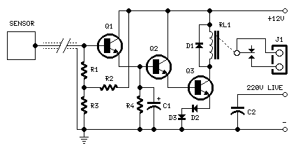
The purpose of this circuit is to animate shop-windows by means of a capacitive sensor placed behind a post-card-like banner. The card is placed against the glass inside the shop-window, and the visitor can activate the relay placing his hand on the card, from the outside. Especially suited for toy-shops, the circuit can activate model trains, small electric racing cars, lights etc. Further applications are left at user's imagination. Adopt it to increase the impact of your shop-window on next Christmas season!
Q1, Q2 & Q3 form a high impedance super-Darlington that drives the relay, amplifying the 50 or 60Hz alternate mains-supply frequency induced in the sensor by the human body. C1, D2 & D3 ensure a clean switching of the relay. Power supply can be any commercial wall plug-in transformer adapter with rectifier and smoothing capacitor, capable of supplying the voltage and current necessary to power the relay you intend to use.
Note: 
  • For proper operation, circuit ground must be connected via a small value, high voltage-rating capacitor to one side of the mains supply socket. The "Live" side is the right one.
Source - http://redcircuits.com/Page22.htm

0 comments

Mosfet Tester Circuit Diagram

Description
This is a variation on the astable multivibrator. Circuit was recently developed to test for N-mosfets(the power kind e.g irf830)
I don’t claim circuit can test all bad mosfets or all fault mosfet conditions. If mosfet is working it will operate in the astable multivibrator circuit causing the Led to flash.
A bad mosfet will not cause the LED to flash.
Below is the circuit diagram, the other half of the astable utilizes an npn transistor to make the circuit cheap.
Almost any npn transistor will work in this circuit.
The npn transistor to the right is used as a common emitter buffer that also drives the led as it receives pulses from the mosfet drain.
Circuit Diagram
 note diode is a light emitting Diode

author: By Tosin Osanyintuyi (TAFRICA)
e-mail: tosinopro@yahoo.com
Source: http://www.electronics-lab.com

0 comments

Two-Tone Siren Circuit Schematic Diagram Using One IC

Description 
 This circuit is intended for children fun, and can be installed on bicycles, battery powered cars and motorcycles, but also on models and various games and toys. With SW1 positioned as shown in the circuit diagram, the typical dual-tone sound of Police or Fire-brigade cars is generated, by the oscillation of IC1A and IC1B gates. With SW1 set to the other position, the old siren sound increasing in frequency and then slowly decreasing is reproduced, by pushing on P1 that starts oscillation in IC1C and IC1D.
The loudspeaker, driven by Q1, should be of reasonable dimensions and well encased, in order to obtain a more realistic and louder output. Tone and period of the sound oscillations can be varied by changing the values of C1, C2, C5, C6 and/or associated resistors. No power switch is required: leave SW1 in the low position (old-type siren) and the circuit consumption will be negligible.
Circuit Schematic Diagram
Parts:

  • R1 = 470K - 1/4W Resistors
  • R2 = 680K - 1/4W Resistor
  • R3 = 470K - 1/4W Resistors
  • R4 = 82K - 1/4W Resistor
  • R5 = 330K - 1/4W Resistor
  • R6 = 10K - 1/4W Resistor
  • R7 = 33K - 1/4W Resistor
  • R8 = 3.3M - 1/4W Resistor
  • C1 = 10µF - 25V Electrolytic Capacitors
  • C2 = 10nF - 63V Polyester Capacitors
  • C3 = 100nF - 63V Polyester Capacitor
  • C4 = 100µF - 25V Electrolytic Capacitor
  • C5 = 10µF - 25V Electrolytic Capacitors
  • C6 = 10nF - 63V Polyester Capacitors
  • D1 = 1N4148 - 75V 150mA Diodes
  • D2 = 1N4148 - 75V 150mA Diodes
  • D3 = 1N4148 - 75V 150mA Diodes
  • Q1 = BC337 - 45V 800mA NPN Transistor
  • P1 = SPST Pushbutton
  • B1 = 6V Battery (4 AA 1.5V Cells in series)
  • IC1 = 4093 - Quad 2 input Schmitt NAND Gate IC
  • SW1 = DPDT Switch
  • SPKR= 8 Ohm Loudspeaker 
Source - http://www.extremecircuits.net/2009/12/two-tone-siren-circuit-schematic-using.html
0 comments

Decibel Meter Circuit Schematic Diagram

Description
The circuit below responds to sound pressure levels from about 60 to 70 dB. The sound is picked up by an 8 ohm speaker, amplified by a transistor stage and one LM324 op-amp section. You can also use a dynamic microphone but I found the speaker was more sensitive. The remaining 3 sections of the LM324 quad op-amp are used as voltage comparators and drive 3 indicator LEDs or incandescents which are spaced about 3dB apart. An additional transistor is needed for incandescent lights as shown with the lower lamp. I used 12 volt, 50mA lamps. Each light represents about a 3dB change in sound level so that when all 3 lights are on, the sound level is about 4 times greater than the level needed to light one lamp. The sensitivity can be adjusted with the 500K pot so that one lamp comes on with a reference sound level. The other two lamps will then indicate about a 2X and 4X increase in volume.
In operation, with no input, the DC voltage at pins 1,2 and 3 of the op-amp will be about 4 volts, and the voltage on the (+) inputs to the 3 comparators (pins 5,10,12) will be about a half volt less due to the 1N914 diode drop. The voltage on the (-) comparator inputs will be around 5.1 and 6.5 which is set by the 560 and 750 ohm resistors.
When an audio signal is present, the 10uF capacitor connected to the diode will charge toward the peak audio level at the op-amp output at pin 1. As the volume increases, the DC voltage on the capacitor and also (+) comparator inputs will increase and the lamp will turn on when the (+) input goes above the (-) input. As the volume decreases, the capacitor discharges through the parallel 100K resistor and the lamps go out. You can change the response time with a larger or smaller capacitor.
This circuit requires a well filtered power source, it will respond to very small changes in supply voltage, so you probably will need a large filter capacitor connected directly to the 330 ohm resistor. I managed to get it to work with an unregulated wall transformer power source, but I had to use 4700uF. It worked well on a regulated supply with only 1000uF. 
 Circuit Schematic Diagram 1
 Circuit Schematic Diagram 2
0 comments

USB Printer Share Switch Circuit Diagram Project

Description 
This simple device allows two computers to share a single USB printer or some other USB device, such as an external flash drive, memory card reader or scanner. A rotary switch selects the PC that you wish to use with the USB device, while two LEDs indicate the selected PC.
The most common way to share a USB printer between two PCs is to use one machine as a print server. However, that’s not always convenient because it means that the server PC must always be on if you want to print something. 
Real Circuit Image
That can be a real nuisance if you just want to quickly fire up the other machine and print something out. It also means that the two PCs must be networked together, either via a hub/router or directly via an ethernet crossover cable.
Another way is to use a dedicated USB print server. However, as before, this must be connected to an ethernet network, along with the PCs. Such devices also need their own power supply, generally cost well over $100 and are overkill if you just want to share a single USB printer between two computers for occasional printing in a home set-up. 
Circuit Layout: 

That’s where this simple device comes in. It’s basically a 2-way switch box that lets you manually switch your USB printer from one PC to the other, as required. The switching is performed using a rotary switch, while two LEDs on the front panel indicate which PC has been connected to the printer.
This method has several advantages. First, you don’t need to network your two computers. Second, you can print from either machine with the other turned off. And third, the device doesn’t need a power supply.
Circuit diagram:
 The circuit uses switch poles S1a-S1c to select either USB socket CON1 or CON2 and connect its pins through to CON3. The fourth pole (S1d) selects either LED1 or LED2, to indicate which PC has been selected.
0 comments

Electromagnetic Field Detector Circuit

Circuit diagram 
This lovely circuit is a real gem! Easy to assemble and more sensitive than many commercial devices available. It's based around an LF351 low-noise operational amplifier and a 1mF choke acting as the sensor. Unlike most other simple EMF detectors, this one has a meter output for accurate reading, but alternatively, you can also roughly estimate the frequency of the field by plugging in headphones. It can detect any field from 50Hz to 100kHz, making it highly versatile and a worthwhile addition to any hobbyist's workbench.
Problems:
 I just couldn't find any.
Possible uses:
 Find out how far electromagnetic fields extend in your room, house, office...
Are you a ghost hunter? Then this is the circuit that you've been waiting for! Since it has been observed that appearance of a ghost tends to disturb the EMF, you can now detect any such changes with this little detector.

Author: Andy Collins' Circuit Exchange
Source - http://www.zen22142.zen.co.uk/
1 comments

Fading Red Eyes Circuit

Description: 
This circuit is used to slowly illuminate and fade a pair of red LEDs (light emitting diodes). The fading LEDs could be installed as 'eyes' in a small pumpkin or skull as a Halloween attraction, or mounted in a Christmas tree ornament. Or, they might be used as a fancy power indicator for your computer, microwave oven, stereo system, TV, or other appliance.
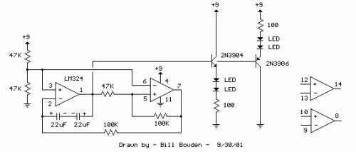
In operation, a linear 3 volt (peak to peak) ramping waveform is generated at pin 1 of the LM1458 IC and buffered with an emitter follower transistor stage. The 22uF capacitor and 47K resistor connected to pin 2 establish the frequency which is about 0.5 Hz. You can make the rate adjustable by using a 100K potentiometer in place of the 47K resistor at pin 2.
The circuit consists of two operational amplifiers (opamps), one producing a slow rising and falling voltage from about 3 volts to 6 volts, and the other (on the right) is used as a voltage comparator, the output of which supplies a alternating voltage switching between 2 and 7 volts to charge and discharge the capacitor with a constant current.
Each of the op-amps has one of the inputs (pins 3 and 6) tied to a fixed voltage established by two 47K resistors so that the reference is half the supply voltage or 4.5 volts. The left opamp is connected as an inverting amplifier with a capacitor placed between the output (pin 1) and the inverting input (pin 2). The right opamp is connected as a voltage comparator so that the output on pin 7 will be low when the input is below the reference and high when the input is higher than the reference. A 100K resistor is connected between the comparator output and input to provide positive feedback and pulls the input above or below the switching point when the threshold is reached. When the comparator output changes at pin 7, the direction of the current changes through the capacitor which in turn causes the inverting opamp to move in the opposite direction. This yields a linear ramping waveform or triangle waveform at pin 1 of the inverting opamp. It is always moving slowly up or down, so that the voltage on the non-inverting input stays constant at 4.5 volts.
Adjustments to the point where the LEDs extinguish can be made by altering the resistor value at pin 3 and 6 to ground. I found a 56K in place of the 47k shown worked a little better with the particular LEDs used. You can experiment with this value to get the desired effect.
Parts List: 

  • Description - Mfg Part# -Allied Part# - Quantity - Cost
  • Operational Amplifier LM1458 - 288-1090 - 1 - .48
  • 47K Resistor - 296-2182 - 4 - .42
  • 100K Resistor - 296-5610 - 1
  • 100 Ohm Resistor - 895-0465 - 1 - .24
  • Transistor 2N3904 - 568-8253 - 1 - .1
  • 22uF Capacitor - 852-6516 - 1 - .07
  • Solderless Breadboard - 237-0015 - 1 - 6.99
  • Red Light Emitting Diode (LED) - 670-1224 - 2 - 0.50
Note: The LED listed has a narrow viewing angle of 30 degrees and appears brightest when looking directly at it. It's not a pure red color, and a little on the orange side, but should be brighter compared to other selections. For a wider viewing angle at reduced intensity, try part number 670-1257 which is viewable at 60 degrees and has a red diffused lens.
Construction details:
 Layout of the solderless breadboard:
Refer to the drawing below the schematic diagram and note the solderless breadboard is arranged in rows labeled A-J, and columns numbered 1 to 65. Each group of 5 holes in the same column are the same connection, so that holes A1,B1,C1,D1 and E1 are all connected together. Likewise holes F1,G1,H1,I1 and J1 are all the same connection. The outer rows along the length of the board are also connected together and are normally used for power supply connections. However, there is a break in the mid section of the outer rows, so a short jumper wire connecting the mid section of the outer rows should be installed to connect the entire outer row together. If you have a DMM, use the low ohms range and probe the various holes to get familiar with the board layout.
Installing the components:
Orientate the LM1458 so the nook or punch mark on one edge is near column 30 and the opposite edge is near column 33. Install the LM1458 on the breadboard so the pins straddle the center section of the board and pin 1 of the IC is occupying hole E30 and pin 8 is in hole F30. The pins are numbered counter clockwise, so pin 4 will be occupying F33 and pin 5 will be in E33. Possible connections for the LM1458, 9 volt battery, and a couple other parts is illustrated in the lower drawing of the solderless breadboard, but it is not complete with all parts.
Refer to the schematic diagram, and install the various other components so they connect to the appropriate pins of the LM1458. Use whatever connection holes are convenient. For example, the 22uF capacitor connects between pins 1 and 2 of the IC, which occupy holes (F30,F31) so it could be placed in the holes (H30, H31) or (J30,J31) or (I30,I31). But not all parts will conveniently fit, so you may have to use a short jumper wire (#22 preferred) to connect parts from one side of the chip to the other.
The board I assembled was connected this way:
  • LM1458 F30 to F33, and E30 to E33
  • 22uF capacitor H30 to H31
  • 47K resistor I30 to I35
  • 47K resistor C27 to C31
  • 47K resistor F25 to Positive battery row
  • 47K resistor J25 to Negative Battery row
  • 100K resistor B31 to B33
  • 2N3904 Transistor G36, G37, G38 with emitter at G38
  • 100 Ohm resistor D38 to F38
  • LED B43 to B44 (Cathode at B44)
  • LED I43 to I44 (Cathode at I43)
  • Jumper A30 to Positive battery row
  • Jumper F36 to Positive battery row
  • Jumper J33 to Negative battery row
  • Jumper J43 to Negative battery row
  • Jumper H25 to J32
  • Jumper J30 to J37
  • Jumper E27 to G31
  • Jumper D32 to G32
  • Jumper D33 to H35
  • Jumper C38 to C43
  • Jumper E44 to F44
  • 9 Volt Battery Postive battery row to negative row.
Circuit diagram
 The circuit below illustrates two pairs of LEDs that operate out of phase so as one pair slowly illuminate, the other pair will fade.
Source - http://www.bowdenshobbycircuits.info/
0 comments
 
Support : Creating Website | Johny Template | Mas Template
Copyright © 2011. The Circuit - All Rights Reserved
Template Created by Creating Website Published by Mas Template
Proudly powered by Blogger